- 您现在的位置:买卖IC网 > Sheet目录479 > MRF89XA-I/MQ (Microchip Technology)TXRX ISM SUB-GHZ ULP 32QFN
�� �
�
�MRF89XA�
�2.10�
�Receiver�
�2.10.1�
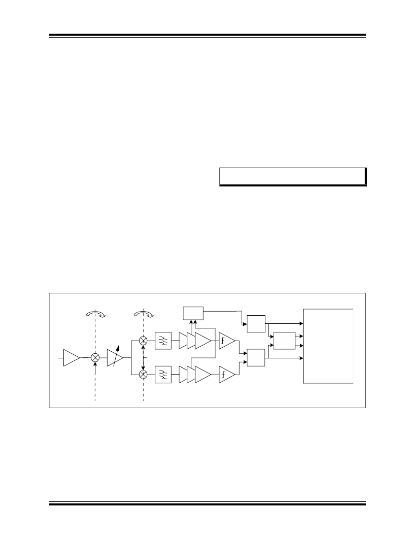
�RECEIVER� ARCHITECTURE�
�The� receiver� is� based� on� a� superheterodyne�
�architecture� and� comprises� the� following� major� blocks:�
�?� An� LNA� that� provides� low-noise� RF� gain� followed�
�by� an� RF� band-pass� filter.�
�?� A� first� mixer,� which� down-converts� the� RF� signal�
�to� an� intermediate� frequency� equal� to� one-ninth� of�
�the� carrier� frequency� (f� rf� 100� MHz� for� 915� MHz�
�signals).�
�?� A� variable� gain� first-IF� preamplifier� followed� by�
�two� second� mixers,� which� down-convert� the� first�
�IF� signal� to� I� and� Q� signals� at� a� low� frequency�
�(zero-IF� for� FSK,� low-IF� for� OOK).�
�?� A� two-stage� IF� filter� followed� by� an� amplifier� chain�
�are� available� for� both� I� and� Q� channels.� Limiters�
�at� the� end� of� each� chain� drive� the� I� and� Q� inputs�
�to� the� FSK� demodulator� function.� An� RSSI� signal�
�is� also� derived� from� the� I� and� Q� IF� amplifiers� to�
�drive� the� OOK� detector.� The� second� filter� stage� in�
�each� channel� can� be� configured� as� either� a� third-�
�order� Butterworth� low-pass� filter� for� FSK� opera-�
�tion� or� an� image� reject� polyphase� band-pass� filter�
�for� OOK� operation.�
�?� An� FSK� arctangent� type� demodulator� driven� from�
�the� I� and� Q� limiter� outputs,� and� an� OOK� demodu-�
�lator� driven� by� the� RSSI� signal.� Either� detector�
�can� drive� a� data� and� clock� recovery� function� that�
�provides� matched� filter� enhancement� of� the�
�demodulated� data.�
�Figure� 2-8� illustrates� the� receiver� architecture� block�
�diagram.� The� first� IF� is� one-ninth� of� the� RF� frequency�
�(approximately� 100� MHz).� The� second� down-�
�conversion� down-converts� the� I� and� Q� signals� to�
�baseband� in� the� case� of� the� FSK� receiver� (zero-IF)� and�
�to� a� low-IF� (IF2)� for� the� OOK� receiver.�
�After� the� second� down-conversion� stage,� the� received�
�signal� is� channel-select� filtered� and� amplified� to� a� level�
�adequate� for� demodulation.� Both� FSK� and� OOK�
�demodulation� are� available.� Finally,� an� optional� bit�
�synchronizer� (BitSync)� is� provided� to� supply� a�
�synchronous� clock� and� data� stream� to� a� companion�
�microcontroller� in� Continuous� mode,� or� to� fill� the� FIFO�
�buffers� with� glitch-free� data� in� Buffered� mode.�
�Note:� Image� rejection� is� achieved� using� a� SAW�
�filter� on� the� RF� input.�
�FIGURE� 2-8:�
�RECEIVER� ARCHITECTURE� BLOCK� DIAGRAM�
�First�
�down-conversion�
�Second�
�down-conversion�
�RSSI�
�OOK�
�Demod�
�BitSync�
�Control� Logic�
�-� Pattern� Recognition�
�-� FIFO� Handler�
�-� SPI� Interface�
�-� Packet� Handler�
�LNA�
�RF�
�LO1� RX�
�IF1�
�LO2� RX�
�FSK�
�Demod�
�Baseband,� IF2� in� OOK�
�?� 2010–2011� Microchip� Technology� Inc.�
�Preliminary�
�DS70622C-page� 21�
�发布紧急采购,3分钟左右您将得到回复。
相关PDF资料
MRF89XAM9A-I/RM
IC TXRX MOD 915MHZ ULP SUB-GHZ
MRX-001-433DR-B
MODULE RECEIVER 433MHZ 18DIP
MRX-002-433DR-B
MODULE RECEIVER 433MHZ 18DIP
MRX-002SL-433DR-B
MODULE RCVR 433MHZ SAW LN 24DIP
MRX-005-915DR-B
MODULE RECEIVER 915MHZ 18DIP
MRX-005SL-915DR-B
MODULE RCVR 915MHZ SAW LN 24DIP
MRX-007-433DR-B
MODULE RECEIVER 433MHZ 18DIP
MRX-008-433DR-B
MODULE RECEIVER 433MHZ 18DIP
相关代理商/技术参数
MRF89XAM8A-I
制造商:MICROCHIP 制造商全称:Microchip Technology 功能描述:Ultra Low-Power, Integrated ISM Band Sub-GHz Transceiver
MRF89XAM8A-I/RM
功能描述:射频模块 868MHz Sub-GHz transceiver module
RoHS:否 制造商:Linx Technologies 产品:Transceiver Modules 频带:902 MHz to 928 MHz 输出功率:- 15.5 dBm to + 12.5 dBm 接口类型:UART 工作电源电压:- 0.3 VDC to + 5.5 VDC 传输供电电流:38.1 mA 接收供电电流:22.7 mA 天线连接器类型:U.FL 最大工作温度:+ 85 C 尺寸:1.15 mm x 0.63 mm x 0.131 mm
MRF89XAM8A-I/RM
制造商:Microchip Technology Inc 功能描述:, Leaded Process Compatible:Yes, Peak Re
MRF89XAM9A_12
制造商:MICROCHIP 制造商全称:Microchip Technology 功能描述:915 MHz Ultra Low-Power Sub-GHz Transceiver Module
MRF89XAM9A-I/RM
功能描述:射频模块 915MHz Sub-GHz Transceiver Mod RoHS:否 制造商:Linx Technologies 产品:Transceiver Modules 频带:902 MHz to 928 MHz 输出功率:- 15.5 dBm to + 12.5 dBm 接口类型:UART 工作电源电压:- 0.3 VDC to + 5.5 VDC 传输供电电流:38.1 mA 接收供电电流:22.7 mA 天线连接器类型:U.FL 最大工作温度:+ 85 C 尺寸:1.15 mm x 0.63 mm x 0.131 mm
MRF89XAM9AT-I/RM
制造商:Microchip Technology Inc 功能描述:915 MHz Ultra Low-Power Sub-GHz Transceiver Module
MRF89XAT-I/MQ
功能描述:射频收发器 868/915/950 MHz Sub-GHz transceiver RoHS:否 制造商:Atmel 频率范围:2322 MHz to 2527 MHz 最大数据速率:2000 Kbps 调制格式:OQPSK 输出功率:4 dBm 类型: 工作电源电压:1.8 V to 3.6 V 最大工作温度:+ 85 C 接口类型:SPI 封装 / 箱体:QFN-32 封装:Tray
MRF8HP21080HR3
功能描述:射频MOSFET电源晶体管 HV8 2.1GHZ 160W NI780H-4 RoHS:否 制造商:Freescale Semiconductor 配置:Single 晶体管极性: 频率:1800 MHz to 2000 MHz 增益:27 dB 输出功率:100 W 汲极/源极击穿电压: 漏极连续电流: 闸/源击穿电压: 最大工作温度: 封装 / 箱体:NI-780-4 封装:Tray